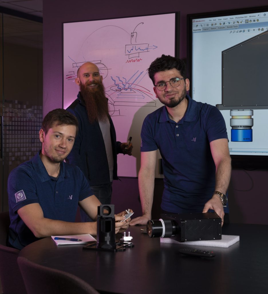
A high-volume direct imaging subsystem
Empowering tomorrow’s PCB and Semicon manufacturing, Visitech’s state-of-the-art direct imaging lithography subsystems are tailor-made for machine builders and tool makers. The Luxbeam Lithography System (LLS) enables you to achieve high-yield manufacturing at high speed without compromising flexibility or increasing the cost of ownership.
Recommended use

Maximum flexibility
for stable, high-yield manufacturing
on the nanometer scale
Incorporate the benefits
The LUXBEAM® Lithography System is for incorporation into direct imaging lithography machines, essentially providing a wide range of valuable benefits that maximize throughput without compromising accuracy, line/width tolerances, your cost of ownership, and manufacturing flexibility.
The ultimate subsystem
Target market segments for the subsystem are PCB lithography and advanced packaging, including Semicon and fine line. Tailor-made to master solder mask, inner layer, outer layer, and advanced packaging alike makes the LLS your ultimate subsystem.

Maximizing flexibility and reducing cost
The manufacturing cost of existing electronics designs for the semiconductor industry is high and lacks flexibility. Further, increasingly stringent requirements apply for more compact layouts including extended functionality in the same die (Moore’s law).
Visitech’s answer to these challenges is advanced packaging using direct imaging, which allows several dies to be interconnected (such as chiplets and System-in-Package (SiP) designs for FOPLP and FOWLP applications). In addition, Visitech’s subsystem enables real-time warping and positioning of the artwork. The subsystem’s combination of software and hardware composes a powerful yet reliable system that maximizes yield.
High-yield manufacturing
We are passionate about meeting our customers’ requirements: High throughput, paired with system stability and continuous innovation, keeps our customers at the cutting edge. In real-time, our systems cope with die-shift, rotation, and trace-connecting from a shifted, rotated, and warped substrate.
The LLS system fully integrates the manipulation of the panel in real-time, which maximizes yield and efficiency over traditional steppers.
APPLICATIONS:
Advanced Packaging
Critical parameters such as stitching, edge roughness, and Critical Dimension (CD) uniformity over wafer and extensive panels, are handled on the nanometer scale. When using System in Package (SiP), System on Chip (SoC), or other advanced packaging methods, the subsystem supports applications such as FOPLP and FOWLP. Real-time warping and positioning of the artwork enable state-of-the-art throughput.
PCB Lithography
High power, speed, and throughput with industry-proven reliability are what machine builders can expect from the LLS subsystem, which provides state-of-the-art specifications for inner/outer layer-resist work and solder mask. In addition, swapping between multiple and configurable wavelength sources is easy.

Controlling the parameters
As a user, you have complete control of the system’s parameters, enabling you to achieve the exact desired geometry of the resist.

World-class software
With our world-class software solution, you get superior quality and throughput from 2,5 µm to 30 µm.

Unparalleled reliability
As fully industrialized products, our systems are field-proven in 24/7 manufacturing environments with excellent reliability. We back this with worldwide service coverage from multiple global locations.

Flexible applications
The LLS system supports a wide array of applications, such as PCB, mSAP, and advanced packaging, yielding the maximum flexibility from your high-throughput subsystem.
Need more details?
We have more information for you! Please get in touch.