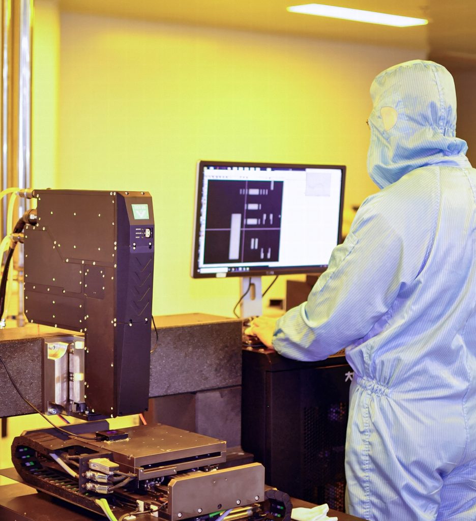
A high-volume direct imaging subsystem
The LLS subsystem is engineered to excel in PCB lithography and advanced packaging, including semiconductor applications and fine-line processes. With tailor-made precision for solder mask, inner and outer layers, and advanced packaging, it delivers unmatched performance—making it the ultimate choice for high-quality, high-efficiency production.

LLS06

LLS04

LLS2500
Maximum flexibility
for stable, high-yield manufacturing
on the nanometer scale

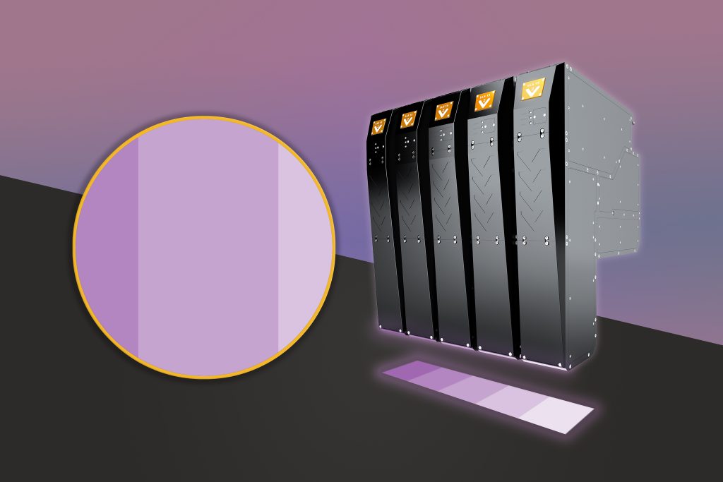
Configurable down to 2 μm
Our system delivers Direct Imaging solutions with resolutions down to 2 μm, allowing customers to configure and optimize for the best balance of quality and throughput within the 2–10 μm range. This flexibility enables our partners to fine-tune their setup to meet mass production process requirements for common line/space specifications, such as 2 μm, 5 μm, and 10 μm—along with any value in between—with nanometer precision.
Throughput
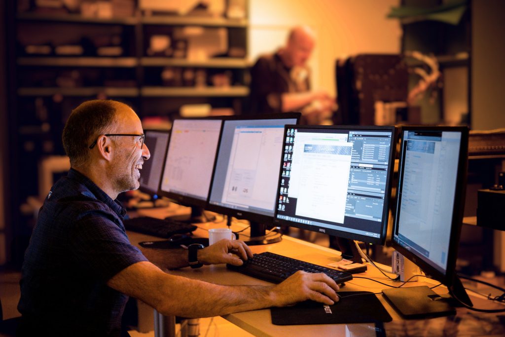
Having developed world-leading light sources, optics, software, and FW for 20 years, our team fine-tunes all parameters for our customers to achieve optimal throughput for a given application requirement, as we understand that this varies heavily depending on the process. Contact us to discuss your throughput needs!


Die-shift
Our next-generation software provides complete flexibility to compensate for die shift and warping challenges in real-time on panels and wafers.
Flexibility
Compatible with wafers, panels, or any other required substrate shape. Equipped with digital data handling and auto-focus features. No panel, package, or reticle size limits.

What stitch?
With Visitech’s proprietary next-generation software, we ensure the absence of stitching effects – regardless of application.
Scalability
Whether your requirement is
- MEMS manufacturing
- Advanced Packaging requiring advanced packaging techniques
- High Density Interconnects
- Flip Chip Ball Grid Array (FCBGA)
- Fan out Panel Level Packaging (FOPLP)
- Fan out wafer level packaging (FOWLP)
- Heterogenous chiplets, Flip Chip Chip Scale Package (FCCSP)
- chip first
- chip last
- organic substrate
… or any other application, contact us for more information on how we can solve your challenges.

Low cost of operation
Visitech photoheads and software provide a low-maintenance, high-throughput, reliable solution with excellent service from our worldwide team of passionate professionals. We will provide you with the necessary resources to ensure uptime.
Explore further
Need more details on our
Fineline/Advanced Packaging products?
We have more information for you! Please get in touch.