Advanced packaging like Fan Out (FO) and System in Package (SiP) is becoming more of a standard to continue the system size-down of small form factor advanced electronic devices, such as mobile phones and smartwatches.
Direct imaging solution for Fan Out Wafer Level Packaging (FOWLP) and Fan Out Panel Level Packaging (FOPLP) and other back end semiconductor applications will enable optimization for the manufacturing process compared to conventional steppers.
In advanced packaging, steppers have limitations in local image warping based on the dies’ actual XY position and rotation.
After registration of the fiducials’ (dies) position, the LLS will in real-time, while printing, warp the image such that the fan-out signal lines are optimized between the dies and the substrate routing. Accurate local registration and LLS real-time local image warping will enable to route more efficiently, with a higher density of signal lines, in the channel between dies pads. This will allow a system design with a smaller footprint which can enable better cooling (battery life before charging is needed.) and, of course, a smaller footprint as such.
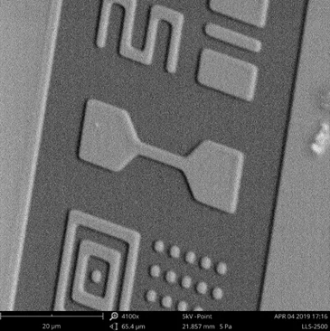
The LLS 2500 is a new photohead in our LLS product line that will print 2 um Line space both on wafer with liquid resist and on PCB with dry resist.
The application must be tested and optimized, but initial testing shows nice printing results in resists up to 12 um height.
Please contact us for further information.

Share


