Visitech is expanding into semiconductor lithography with the launch of a 1µm L/S capable system – the LLS1000. New direct imaging equipment built for fan-out wafer-level packaging (FOWLP), fan-out panel-level packaging (FOPLP), and advanced packaging applications. The LLS1000 is a direct imaging subsystem, designed from the ground up for toolmakers serving the semiconductor industry – compatible with both 405nm and 375nm resist applications.
A new architecture, not an update
The LLS1000 is a distinct product line, developed around a new optical and electronics architecture rather than a revision of existing designs. As a lithography system, it introduces a new lens, a 4K DLP optical and electronic architecture, including new laser light sources – positioning the LLS1000 as laser direct imaging equipment and laying the groundwork for the next generation of Visitech’s UV light engines for machine builders.
The result is a system designed for 1µm line/space resolution, built to support the tighter tolerances and higher functional density that advanced packaging formats such as chiplets and SiP design require. The LLS1000 enables tool makers to viably use direct write/imaging as an alternative to steppers, scanners, and mask aligners for 1µm CD resolution.
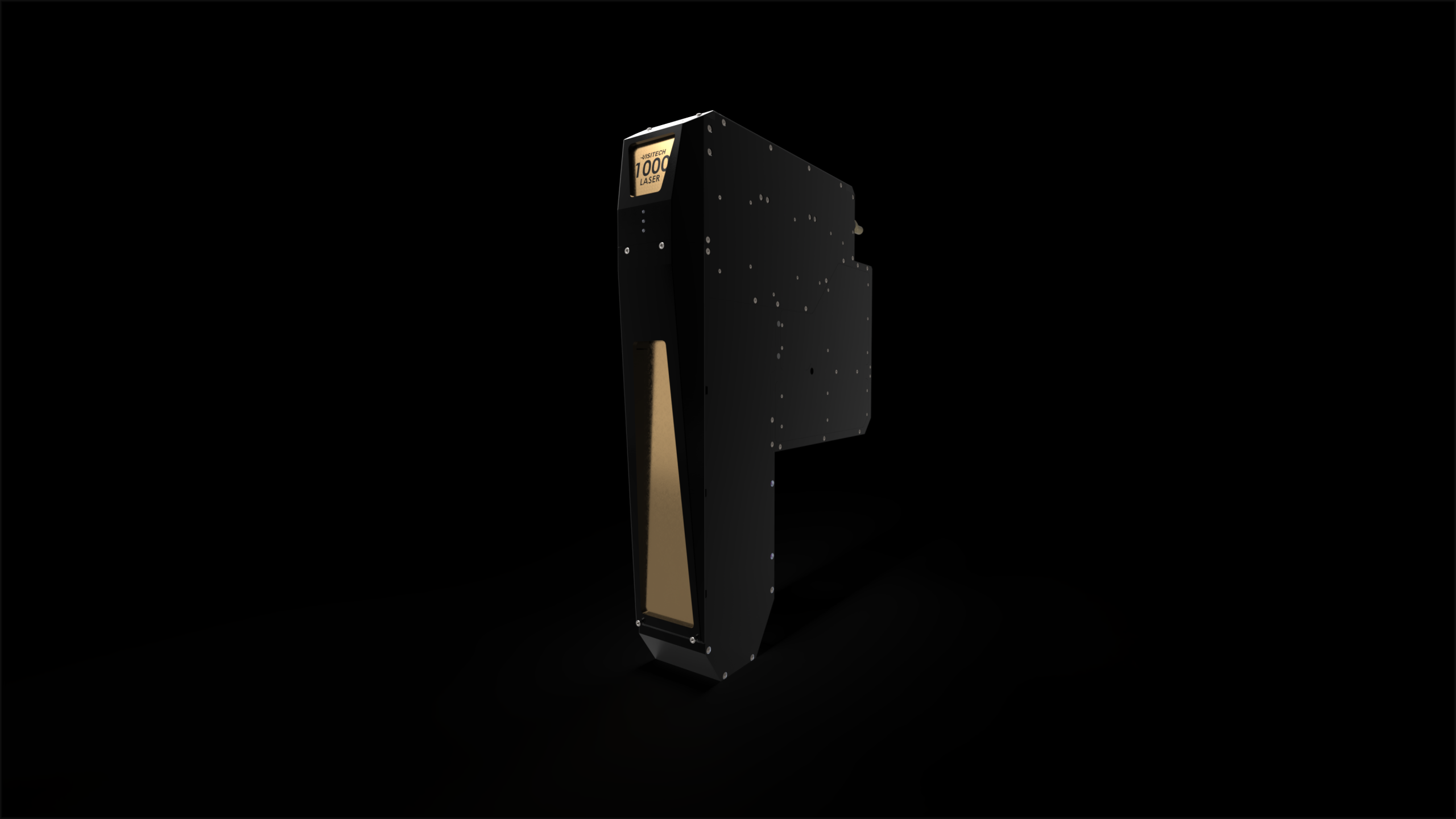
LLS1000 product render
Built for throughput, not just precision
Fine feature resolution alone does not solve the packaging industry’s core challenge: manufacturing cost and flexibility. The LLS1000 is designed as a true high-throughput maskless lithography system, part of Visitech’s growing range of high-throughput subsystems aimed at production environments rather than prototyping alone.
This is supported by a new generation of Visitech’s operating software, offering:
- Industrial-level throughput at 1µm CD resolution
- Stitch-free exposure across the full imaging field
- Positional warping compensation
- Panel warping compensation
Together, these give machine builders and tool makers greater process freedom, with the goal of high yield, high throughput, and robust operation on the production floor.
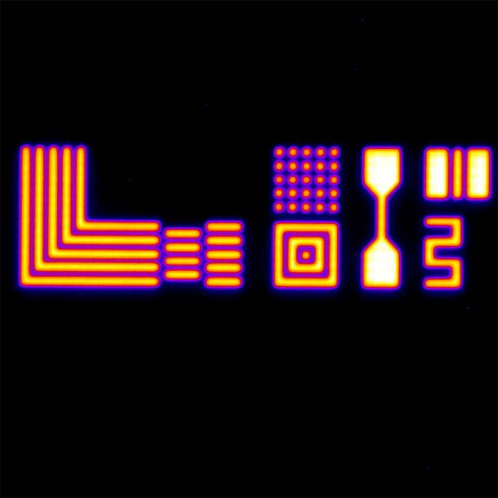
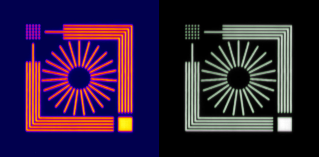
Print comparison and resolution
What does this mean for the industry
Semiconductor manufacturers and tool makers are under growing pressure to pack more functionality into smaller packages, while keeping production costs under control. Direct imaging lithography, replacing conventional mask-based exposure, is one of the clearest paths to meeting that pressure without sacrificing flexibility, whether the target is wafer direct imaging or panel-based advanced packaging formats.
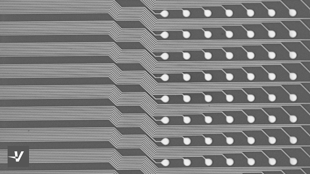
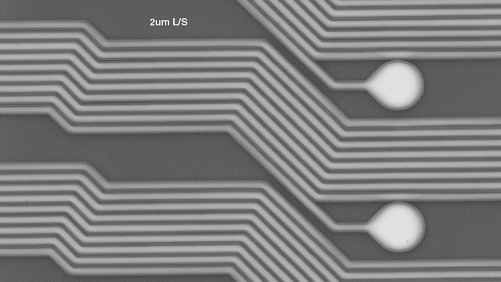
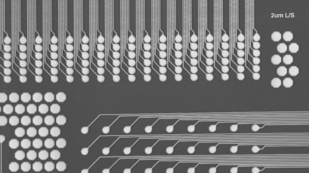
RDL interconnect routing
The LLS1000 extends this approach into direct imaging semicon applications specifically, bringing direct laser lithography to a segment where existing exposure methods struggle to keep pace with shrinking line widths.
With the LLS1000, Visitech brings its DLP subsystem expertise, built over more than a decade in PCB and advanced packaging, into a platform purpose-built for semiconductor applications.
Share