
Direct Imaging · Advanced Packaging
A high-volume direct imaging subsystem
For advanced packaging — fan-out, RDL, bumping and chiplet interconnect, on wafer and panel. Maskless Direct Imaging configurable down to 1 µm line/space, with real-time die-shift compensation and stitch-free imaging.
Direct Imaging in motion Direct Imaging in volume production Built for the fab floor Assembled and tested in-house
Why LUXBEAM® for ADVANCED packaging
A subsystem built for high-volume packaging
Configurable resolution
Direct Imaging configurable across the packaging range — line/space from 6 µm down to 1 µm, matched to your process.
Throughput, tuned
Exposure parameters optimised for the throughput your application needs — tell us the substrate and volume, and we spec to it.
Die-shift compensation
Next-generation software compensates for die shift and warping in real time — on panels and wafers alike.
Stitch-free imaging
Proprietary software removes stitching artefacts entirely — regardless of pattern or substrate size.
Substrate flexibility
Wafers, panels or any required substrate shape — digital data handling and auto-focus, with no fixed size limits.
Low cost of operation
A low-maintenance, high-throughput, reliable subsystem — backed by worldwide support.
Scalability
One subsystem, many processes
The same LUXBEAM® heads scale across packaging and semiconductor-adjacent processes:
Recommended photoheads
Heads for advanced packaging
Five photoheads cover the packaging range, from 6 µm down to 1 µm line/space. Start from the finest line you need to draw, or compare them all in the full spec table.
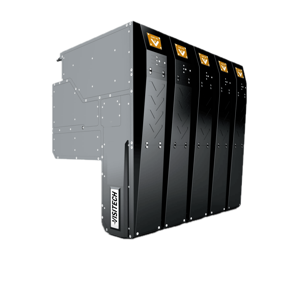
lls photoheads suitable for advanced packaging
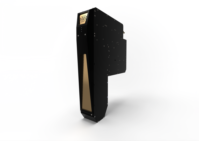
LLS1000
1µmLine / space- Source
- 405 / 375 nm laser
- Ø300 wafer
- ~32 s · 112 wph
- Panel
- ~110 s/side · 32 pph
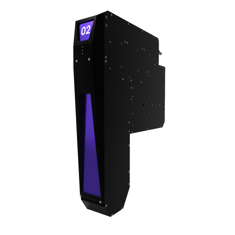
LLS02
2µmLine / space- Source
- 405 / 375 nm laser
- Ø300 wafer
- 60 wph
- Panel
- 20 pph
LLS03
3µmLine / space- Source
- 405 / 375 nm laser
- Ø300 wafer
- 102 wph
- Panel
- 32 pph
LLS05
5µmLine / space- Source
- 405 / 375 nm laser
- Ø300 wafer
- 132 wph
- Panel
- 85 pph
LLS06
6µmLine / space- Source
- 405 / 375 nm laser, or 4-peak LED
- Ø300 wafer
- 720 wph
- Panel
- 240 pph
Imaged in production
Packaging lines, actually imaged
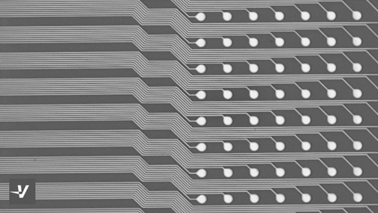
Real microscopy of resist patterned by LUXBEAM® photoheads on packaging substrates — no renders. Open any tile to see the full frame.
Resist · Microscopy 2 µm L/S
LLS02 · Wafer 2 µm L/S
LLS03 · Optical 3 µm L/S
LLS1000 · detail < 1 µm edge
Which packaging processes does the LUXBEAM® subsystem cover?
The same heads scale across fan-out (FOPLP/FOWLP), RDL, bumping and heterogeneous chiplet interconnect, plus HDI, FCBGA and MEMS. They image on both wafer and panel, and on chip-first or chip-last flows.
What is the finest line/space you can image?
For advanced packaging, the photoheads run from 6 µm down to 1 µm line/space, configured to your process. The finest head in the range is the LLS1000 at 1 µm. It writes the finest RDL for CPO and photonic interposers, and glass-core fine RDL.
Why maskless direct imaging instead of a mask?
Maskless imaging works directly from digital data, so there is no mask cost and patterns change instantly between jobs. It also lets the software compensate for die shift and warping in real time and image stitch-free — neither of which a fixed mask can do.
How is throughput determined?
Throughput depends on the head, the resolution and the substrate format. As a guide on Ø300 wafers, LLS06 reaches 720 wph at 6 µm and LLS02 runs 60 wph at 2 µm. Tell us the substrate and volume and we spec the exposure to it.
Which photohead suits my application?
Five photoheads cover the packaging range: LLS06 (6 µm), LLS05 (5 µm), LLS03 (3 µm), LLS02 (2 µm) and LLS1000 (1 µm). Start from the finest line you need to draw, then compare them in the full spec table.
Can it integrate as an OEM subsystem in our machine?
Yes — the photoheads are designed as a direct imaging subsystem to build into your platform, with digital data handling and auto-focus and no fixed substrate-size limits. It’s a low-maintenance, reliable building block backed by worldwide support.
Get started
Bring maskless packaging into your line
Tell us the substrate, the target line/space and the format — we’ll come back with a recommended photohead and a configuration, usually within two business days.