
LUXBEAM® Lithography System
Maskless lithography.
From 30 µm down to 1 µm.
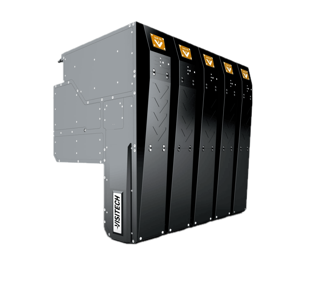
We engineer the imaging heart inside your machine: DLP®-based Direct Imaging, built in-house from optics to firmware.
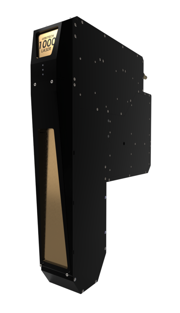
Introducing LLS1000
1 µm L/S
The smallest line we’ve ever drawn. A LASER photohead built for 1 µm production, without sacrificing throughput.
- Ø300 mm wafer
- 112 wafers/hour
- 510×515 mm panel
- 32 panels/hour
- Light source
- LASER
Choose your photohead
One maskless DLP platform covers PCB soldermask at 30 µm down to 1 µm advanced packaging: the LUXBEAM® LLS photoheads, across two segments. Pick by application; we’ll spec by resist, panel and target line/space.
PCB · Inner & Outer Layer
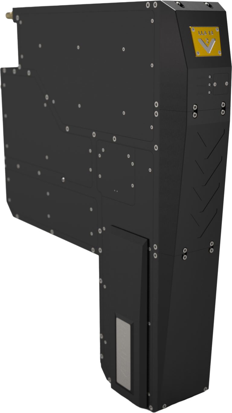
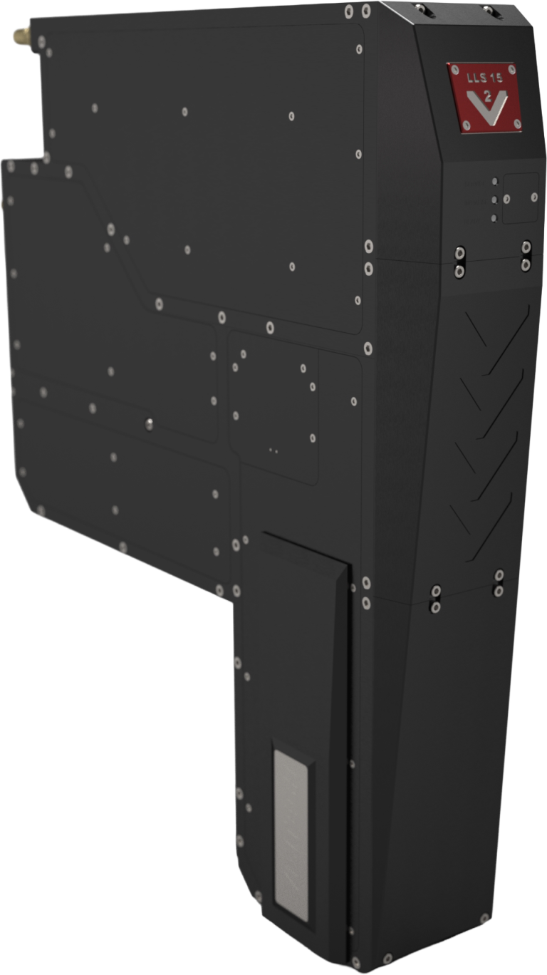
LLS15
15µmLine / space- Source
- 405 nm (h-line) laser, or 4-peak LED
- Throughput
- ~8 s/side
- Substrate
- 510×515, 600×600, large PCB
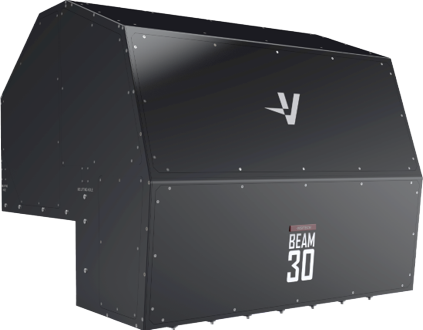
BEAM30
30µmLine / space- Source
- 1–7 channel 4-peak LED
- Throughput
- ~9.5 s/side
- Substrate
- Largest panels, high power
LLS30
30µmLine / space- Source
- 405 nm (h-line) laser, or 4-peak LED
- Throughput
- ~8 s/side
- Substrate
- Largest production panels
Fineline · Advanced Packaging · Semicon
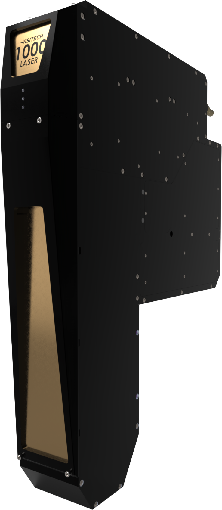
LLS1000
1µmLine / space- Source
- 405 nm (h-line) / 375 nm (i-line) laser
- Ø300 wafer
- ~32 s · 112 wph
- Panel
- ~110 s/side · 32 pph
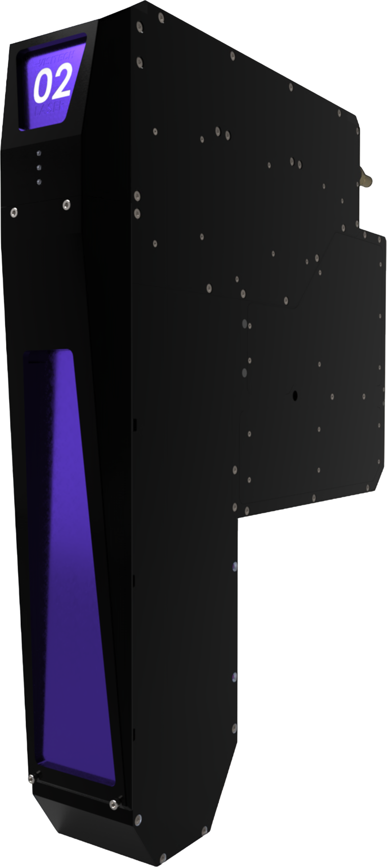
LLS02
2µmLine / space- Source
- 405 nm (h-line) / 375 nm (i-line) laser
- Ø300 wafer
- 60 wph
- Panel
- 20 pph
LLS03
3µmLine / space- Source
- 405 nm (h-line) / 375 nm (i-line) laser
- Ø300 wafer
- 102 wph
- Panel
- 32 pph
LLS05
5µmLine / space- Source
- 405 nm (h-line) / 375 nm (i-line) laser
- Ø300 wafer
- 132 wph
- Panel
- 85 pph
LLS06
6µmLine / space- Source
- 405 nm (h-line) / 375 nm (i-line) laser, or 4-peak LED
- Ø300 wafer
- 720 wph
- Panel
- 240 pph
Print testing on wafer
Real resist, patterned by Visitech photoheads
No simulations, no marketing renders. Real microscopy of resist patterned by Visitech photoheads, straight from the production floor. Open any tile to see the full frame.
LLS1000 · Wafer 1 µm L/S
LLS02 · Wafer 2 µm L/S
LLS03 · Wafer 3 µm L/S
LLS1000 · detail Resist edge
Why maskless
Masks are the past.
Direct imaging is the future.
Traditional mask-based lithography ties you to rigid workflows: every design change means a new physical mask, adding cost, lead time, and waste. Maskless direct imaging entirely eliminates this bottleneck.
With Visitech’s direct imaging, the pattern is data and not a mask. High-mix runs with no tooling or changeover, at any volume. The warping engine corrects every exposure in real time, scaling, shifting, rotating and distorting the pattern to cancel panel distortion, die shift and process warp. You pattern to where the features actually are, not where they were meant to be.
Zero mask
No physical masks to procure, store, inspect, or replace. Every design iteration is free.
Instant design changes
Digital artwork means zero turnaround. Change your layout and expose immediately.
Higher yield
Real-time warping compensates for substrate variation, maximizing first-pass yield.
Lower cost of ownership
LED and laser diode sources deliver superior lifetime with minimal maintenance.
Everything is built in-house
Visitech designs, engineers, manufactures, and tests every critical element under one roof. Optics, electronics, light sources, software, firmware, and hardware. This means tighter tolerances, faster iteration, and complete system-level optimization.
Imaging
Heart
Field Proven – worldwide
Few direct-imaging platforms cover both ends of electronics manufacturing. Ours does: from cost-driven, high-throughput PCB to high-value packaging and IC substrates, and it’s already running 24/7 in production worldwide.
Inner & Outer Layer PCB
High-throughput Direct Imaging for soldermask and inner/outer-layer patterning, LED and LASER, down to 15 µm fine-line.
Fineline, Packaging & IC
Fan-out and high-density RDL down to 1 µm line/space. LASER photoheads built for wafer and panel, with the warping engine that holds overlay across a distorted panel.
Semiconductors & IC Substrates
IC substrate, glass core and wafer-level MEMS and mask writing, from 6 µm down to 1 µm line/space.

Engineered in-house.
Deployed and supported worldwide.
- Years of DLP experience
- 25+
- Finest line / space
- 1 µm
- Field-proven reliability
- 24/7
What is maskless lithography / direct imaging?
Maskless lithography exposes patterns directly onto a substrate without physical masks. The image is generated digitally and projected through DLP®-based optics, enabling rapid design changes, flexible workflows and elimination of mask-related costs and lead times.
How does DLP-based imaging compare to laser direct imaging?
DLP-based systems expose entire patterns in parallel, while laser systems typically scan point-by-point. Depending on application and resolution, this can provide advantages in throughput and scalability.
Do you deliver complete systems?
No. Visitech provides the lithography subsystem (the LUXBEAM® photohead plus LURIA control software). Complete systems are delivered with partners who integrate motion, handling and process equipment around the exposure system.
What applications are supported?
PCB and advanced packaging, semiconductor-related processes, microfabrication and MEMS, and additive manufacturing (photopolymer-based processes). Each system is configured to the required resolution, substrate, resist and throughput.
Bring Visitech inside your next machine
Tell us about the resist, the panel, the line / space and the volume — we’ll come back with a configuration and a timeline.
- NorwayHQ · Drammen
- ChinaShanghai
- United StatesAllen, TX
- JapanTokyo