
Direct Imaging · Semiconductors & IC Substrates
Maskless imaging for IC substrates and wafer-level work
For IC substrate build-up, mSAP fine-line and glass core, and for wafer-level MEMS, sensors and mask writing. Direct Imaging from 6 µm down to 1 µm line/space, on panels up to 600 × 600 mm and on wafers.
Direct Imaging in motion Direct Imaging in volume production Built for the fab floor Assembled and tested in-house
Why LUXBEAM® for substrates and semiconductor
Process control across the full panel
Fine-line on large panels
IC substrate, interposers and RDL, mSAP fine-line, and glass build-up at 5 to 6 µm line/space, on panels up to 600 × 600 mm.
1 µm on wafers and glass
LLS1000 writes 1 µm line/space on wafers and glass, for glass-core fine RDL and mask writing.
CD control over the whole format
Stitching, edge roughness and CD uniformity are controlled across the whole format. CD uniformity is above 90 % across wafer and panel.
Real-time warp compensation
LURIA reads the substrate before every exposure and adapts the artwork to panel shift, rotation, expansion and warpage.
i-line compatible
The 375 nm laser option gives i-line resist compatibility and the finest features.
Fab-ready data
GDSII and OASIS input, unit-level serialization and full API access. The head fits the fab software you already run.
Applications
From substrate build-up to wafer-level
The same LUXBEAM® platform covers substrate manufacturing and wafer-level semiconductor processes:
Recommended photoheads
Heads for substrates and semiconductor
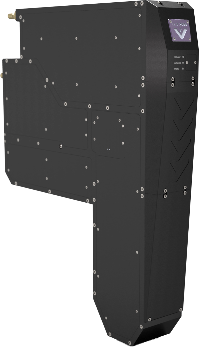
Five photoheads cover this range, from 6 µm down to 1 µm line/space. LLS05 and LLS06 carry IC substrate and glass build-up on panels up to 600 × 600 mm. LLS03 takes IC substrate and RDL at 3 µm. LLS02 and LLS1000 take glass core and wafer-level work. Compare them all in the full spec table. Figures are for discussion and to be confirmed per application.
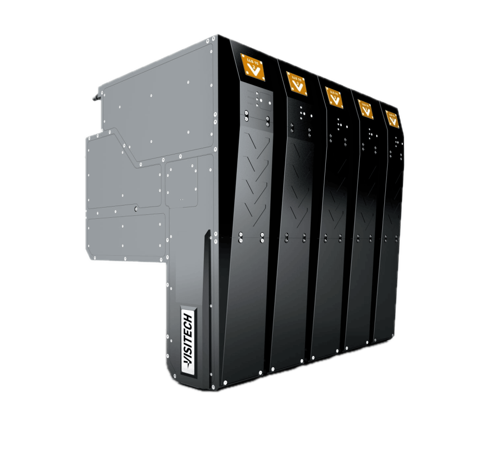
lls photoheads suitable for substrates and semiconductor
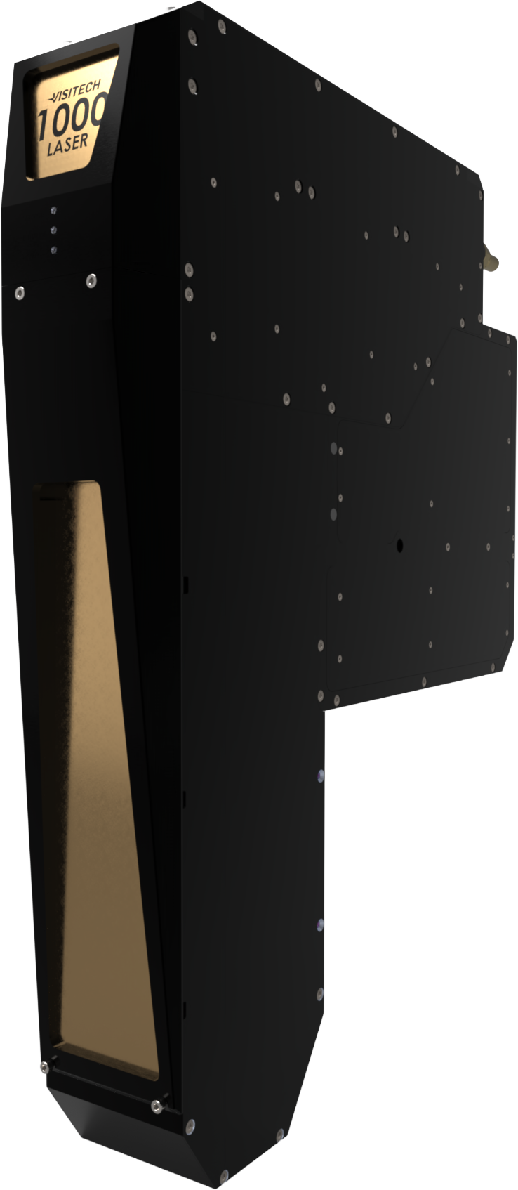
LLS1000
1µmLine / space- Source
- 405 nm (h-line) / 375 nm (i-line) laser
- Ø300 wafer
- ~32 s · 112 wph
- Panel
- ~110 s/side · 32 pph
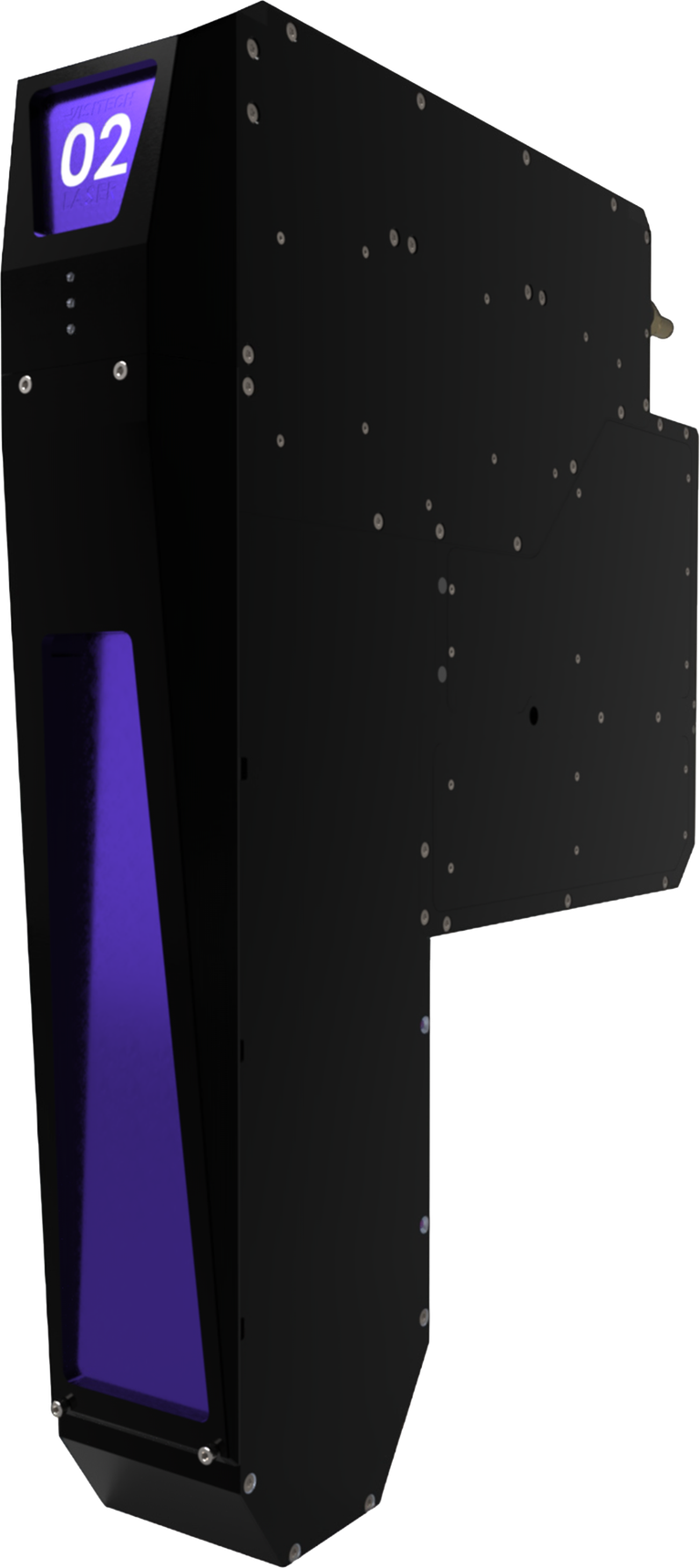
LLS02
2µmLine / space- Source
- 405 nm (h-line) / 375 nm (i-line) laser
- Ø300 wafer
- 60 wph
- Panel
- 20 pph
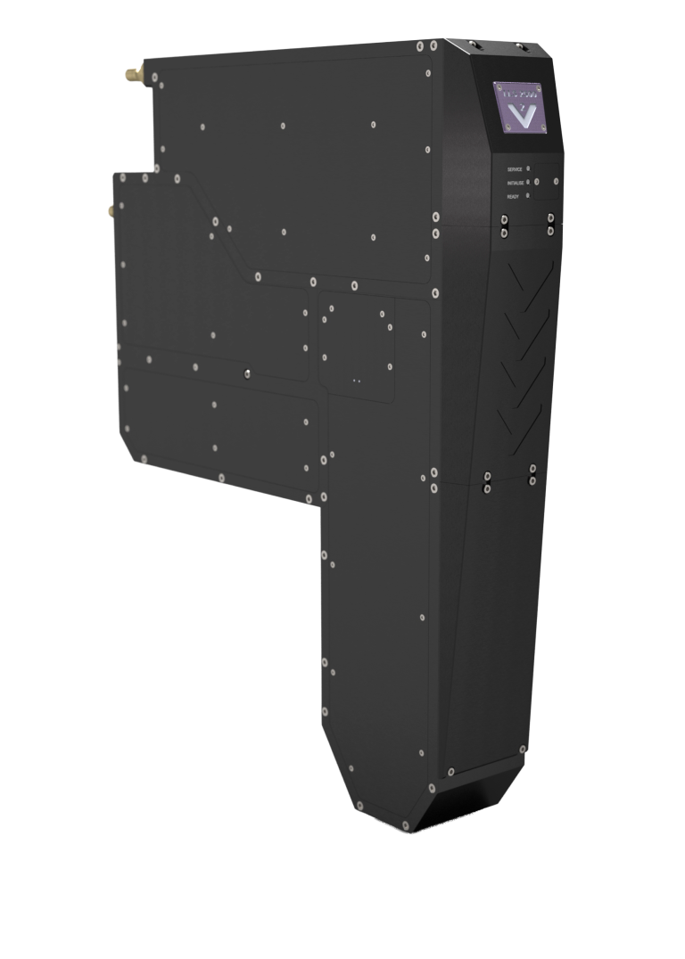
LLS03
3µmLine / space- Source
- 405 nm (h-line) / 375 nm (i-line) laser
- Ø300 wafer
- 102 wph
- Panel
- 32 pph
LLS05
5µmLine / space- Source
- 405 nm (h-line) / 375 nm (i-line) laser
- Ø300 wafer
- 132 wph
- Panel
- 85 pph
LLS06
6µmLine / space- Source
- 405 nm (h-line) / 375 nm (i-line) laser, or 4-peak LED
- Ø300 wafer
- 720 wph
- Panel
- 240 pph
Imaged in production
Fine lines, actually imaged
Real microscopy of resist patterned by LUXBEAM® photoheads. No renders. Open any tile to see the full frame.
Resist · Microscopy 2 µm L/S
LLS02 · Wafer 2 µm L/S
LLS03 · Optical 3 µm L/S
LLS1000 · detail Resist edge
Which substrate and semiconductor processes does the LUXBEAM® subsystem cover?
IC substrate build-up (FCBGA, FCCSP), interposers and RDL, mSAP fine-line, SLP and glass build-up on panels, plus glass core, HBM RDL and wafer-level work such as MEMS, sensors, microfluidics and mask writing. All heads run on the same LURIA platform.
What line/space can you image on IC substrate?
LLS05 and LLS06 cover IC substrate, mSAP fine-line and glass build-up at 5 to 6 µm line/space, on panels up to 600 × 600 mm. For finer RDL and interposers, LLS03 goes to 3 µm, and LLS02 and LLS1000 take it to 2 and 1 µm.
Which panel and wafer formats are supported?
Panels at 310 × 310, 510 × 515 and 600 × 600 mm. LLS1000, LLS02 and LLS03 also image on wafers, and LLS1000 on glass. The subsystem sets no theoretical limit on panel size; the format is set by the machine it is built into.
How do you handle warpage and die shift?
LURIA reads the substrate before every exposure and adapts the artwork in real time: positioning, scaling, rotation and warping, plus die-shift compensation and interconnect re-routing. That keeps feature placement accurate where a rigid mask falls short.
Which resists and wavelengths can I use?
LLS1000 to LLS05 use a 405 nm (h-line) / 375 nm (i-line) laser; the 375 nm option gives i-line resist compatibility. LLS06 can also run a 4-peak LED at 365, 380, 395 and 405 nm, switchable per process.
Can the photoheads be built into our own equipment?
Yes. The LLS is a subsystem for tool makers: liquid-cooled photoheads, GDSII, OASIS, ODB++ and Gerber input, full API access and parameter control, and autofocus that runs on the subsystem or feeds your motion controller.
Get started
Bring maskless imaging to your substrate line
Tell us the substrate, the target line/space and the panel or wafer format — we’ll come back with a recommended photohead and a configuration, usually within two business days.