
lithography · custom applications
Proven platform, configured to your process
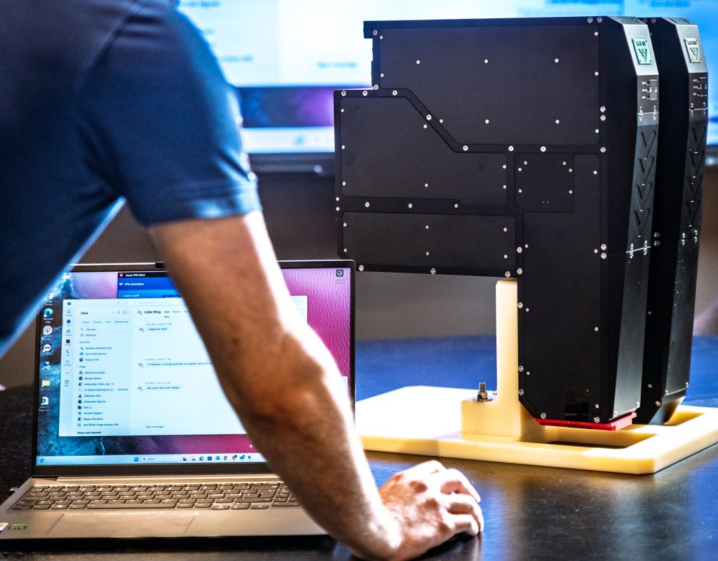
We start from the platform behind our PCB, advanced packaging and semicon photoheads, and configure it to your substrate, your stack, your line / space. Tell us the imaging challenge and we’ll spec it.
Where standard configurations fall short
Substrate, exposure, process or scale: any one of these can take a requirement beyond the standard lineup. None takes it beyond the platform. Describe the constraint and we will specify a configuration around it.
-
Non-standard substrates
Materials, thicknesses or surface topographies outside normal panel and wafer handling.
-
Atypical exposure requirements
Resist chemistries, layer counts or wavelength needs that sit between our defined segments.
-
Hybrid processes
Imaging combined with another production step, where the exposure has to fit an existing line rather than the other way around.
-
Constraints of scale
Footprint, throughput or cost targets that rule out a standard system configuration.
How it works
- You describe the imaging challenge. What is the result your process has to achieve?
- We assess it against the platform. With photoheads ranging from 30 µm to 1 µm, with the optics, electronics and software developed in-house, means most of the variables are ours to move.
- We run a test exposure. Real resist, real microscopy, on your material where possible.
- You get a specified configuration. Photohead, software and integration path, with figures confirmed for your application.
Get started
Need more details? Let’s talk
Tell us what you need — we’ll come back with a configuration, the options and a timeline.
- NorwayHQ · Drammen
- ChinaShanghai
- United StatesAllen, TX
- JapanTokyo