
LUXBEAM® LLS1000
Maskless Direct Imaging, below 1 µm
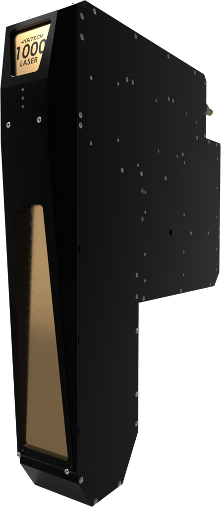
LLS1000 brings DLP-based direct imaging into the sub-micron node — the resolution semiconductor-adjacent and advanced-packaging lines need, at production throughput. One photohead, integrated into your machine, built in-house from optics to firmware.
In production
Sub-micron, in real production
The LLS1000 maintains 1 µm line/space resolution at full production throughput. The complete imaging system – from optics to firmware – is in production and shipping today.
What sets it apart
-
Sub-micron resolution
A LASER source and high-NA projection optics resolve down to 1 µm line/space — the sub-micron node semicon-adjacent and advanced-packaging lines demand, at production throughput.
-
Stitch-free, in focus
Real-time autofocus and stitch-free imaging hold sub-micron features across the full field — verified by SEM on production resist.
-
Vertically integrated
Optics, LASER source, DMD, electronics and the LURIA software stack — engineered under one roof and delivered as one imaging head you mount and drive.
Applications
Where LLS1000 fits
Sub-µm semicon
1 µm line/space on Ø300 wafers for semiconductor-adjacent patterning — MEMS, sensors and emerging device nodes where masks are too slow to iterate.
Advanced packaging
The finest packaging lines — fan-out, RDL and chiplet interconnect — exposed maskless, with die-shift compensation and stitch-free imaging built in.
R&D to production
Change the design at 2 PM, run it at 3 PM. The same photohead carries a process from first silicon through to 24/7 production volume.
Print testing — on wafer
Sub-µm imaging, actually imaged
No simulations, no marketing renders. Real microscopy of resist patterned by LLS1000 — straight from the production floor. Open any tile to see the full frame.
LLS03 · Optical 3.0 µm
LLS02 · SEM 2.0 µm
LLS1000 · Si wafer · SEM 1.0 µm
LLS1000 · detail · SEM < 1 µm edge
Specifications
LLS1000 — at a glance
Imaging & Layout
- Resolution
- 1 µm
- Light source
- 405 / 375 nm laser
- Throughput — Ø300 mm wafer
- ~32 s · 112 wph
- Throughput — 515 × 510 mm panel
- ~110 s/side · 32 pph
- Test substrate
- Resist
- Typical applications
- Finest RDL for CPO and photonic interposers, glass-core fine RDL, mask writing
- Substrate / panel
- Wafers, up to 600×600, glass
- Segment
- Advanced packaging
Integration
- Mechanical mount
- OEM-defined kinematic
- Cooling
- Liquid
- Power
- 24 V DC + aux
- Control interface
- Ethernet (LURIA) · GPIO
- Data path
- 10 GbE pattern streaming
- Pattern formats
- GDSII · OASIS · ODB++ · Gerber
- Real-time features
- Positioning · scaling · rotation · warping · re-routing · autofocus
- Operating environment
- Class 1000 · 22±2 °C · 45±5 % RH
Throughput measured single-pass on Ø300 mm resist; panel figures on 515×510 mm. Real-world numbers depend on resist and energy density — consult the datasheet for verified values under your process.
Why Visitech
We engineer the imaging heart
inside your next machine
Masks are the past
Maskless DLP-based exposure means zero physical masks to procure, store or replace. Change the design at 2 PM, run production at 3 PM.
Vertically integrated
Every critical element under one roof — tighter tolerances, faster iteration and complete system optimisation that bolt-together solutions cannot match.
Field-proven partner
The industry standard for high-throughput Direct Imaging — running 24/7 in PCB, advanced packaging and semicon production worldwide.

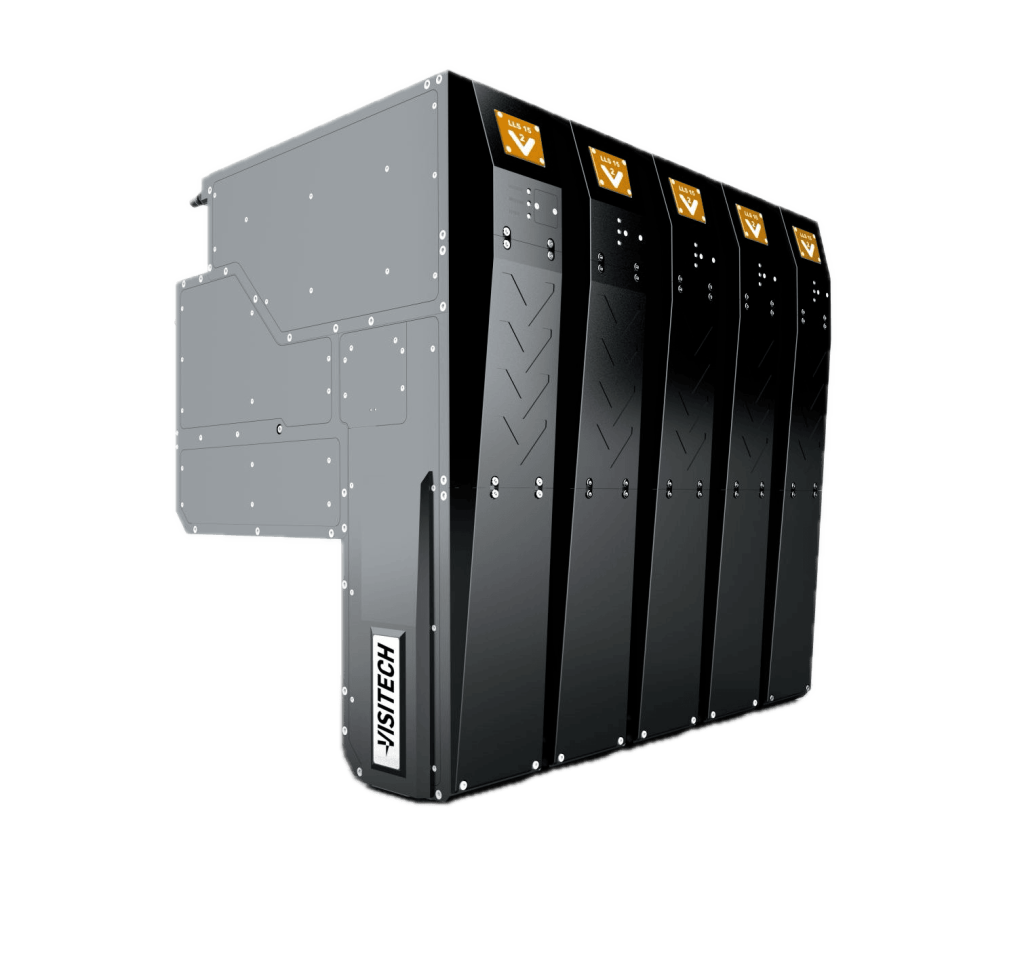
Engineered in-house.
Deployed and supported worldwide.
- Years of DLP experience
- 25+
- Systems deployed
- 15 000+
- Field-proven reliability
- 24/7
What is the LLS1000?
The LLS1000 is the flagship LUXBEAM® photohead — a maskless, DLP-based Direct Imaging subsystem that exposes patterns down to 1 µm line/space. It is a subsystem you integrate into your own machine, not a complete tool.
How does it reach 1 µm?
A LASER light source and high-NA projection optics drive a DMD micromirror array, with real-time autofocus and stitch-free imaging holding sub-micron features across the field — verified by SEM on production resist.
Subsystem or complete system?
A subsystem. Visitech delivers the imaging heart — optics, light source, DMD, electronics and the LURIA software stack — which you mount and control via Ethernet and GPIO in your own platform.
What throughput can I expect?
~112 wafers/hour on Ø300 mm (single pass) and ~32 panels/hour on 515×510 mm. Real-world throughput depends on your resist and energy density — the specification above lists the measured conditions.
When is it available?
LLS1000 is pre-production, entering production in 2026. Talk to an engineer to reserve an evaluation slot and discuss integration timelines for your platform.
Get started
Bring Visitech inside your next machine
Tell us about the resist, panel, line/space, and volume you need — we’ll come back with a configuration and timeline.
- NorwayHQ · Drammen
- ChinaShanghai
- United StatesAllen, TX
- JapanTokyo