
LUXBEAM® LLS06
6 µm, at 720 wafers an hour
Where fineline PCB and advanced packaging meet: 6 µm line and space from a 405 / 375 nm laser or a 4-peak LED, at the highest throughput in the fine end of the lineup.
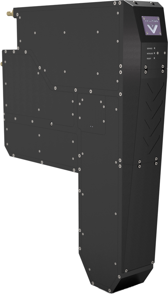
What sets it apart
LLS06 — in three numbers
-
6 µm line and space
Above 90% CD uniformity, with the alignment camera as an option rather than a fixture.
-
Laser or 4-peak LED
405 / 375 nm laser, or a switchable 365 / 380 / 395 / 405 nm LED — the first head in the range where the source is a real choice.
-
720 wafers an hour
Or 240 panels an hour on 515 × 510 mm. Volume-line throughput at 6 µm.
Application fit
Where LLS06 fits
Selective advanced packaging
The fine layers of an AP stack, where only some of the panel needs this resolution.
IC substrate and glass build-up
Build-up layers on organic and glass cores, at panel scale.
mSAP SLP
Substrate-like PCB by modified semi-additive process.
HBM RDL
Redistribution for high-bandwidth memory stacks.
Specifications
LLS06 — at a glance
Imaging & Layout
- Resolution
- 6 µm
- Light source
- 405 / 375 nm laser, or 4-peak LED
- Throughput — Ø300 mm wafer
- 720 wph
- Throughput — 515 × 510 mm panel
- 240 pph
- Typical applications
- Selective AP, IC substrate / glass build-up, mSAP SLP, HBM RDL
- Substrate / panel
- 310×310, 510×515, 600×600
- Segment
- AP / fine-line PCB
Integration
- Cooling
- Liquid
- Pattern formats
- GDSII · OASIS · ODB++ · Gerber
- Real-time features
- Positioning · scaling · rotation · warping · re-routing · autofocus
Figures are for discussion and to be confirmed per application. Throughput depends on resist and energy density — send us both and a field application engineer will verify them for your process.
Why Visitech
We engineer the imaging heart
inside your next machine
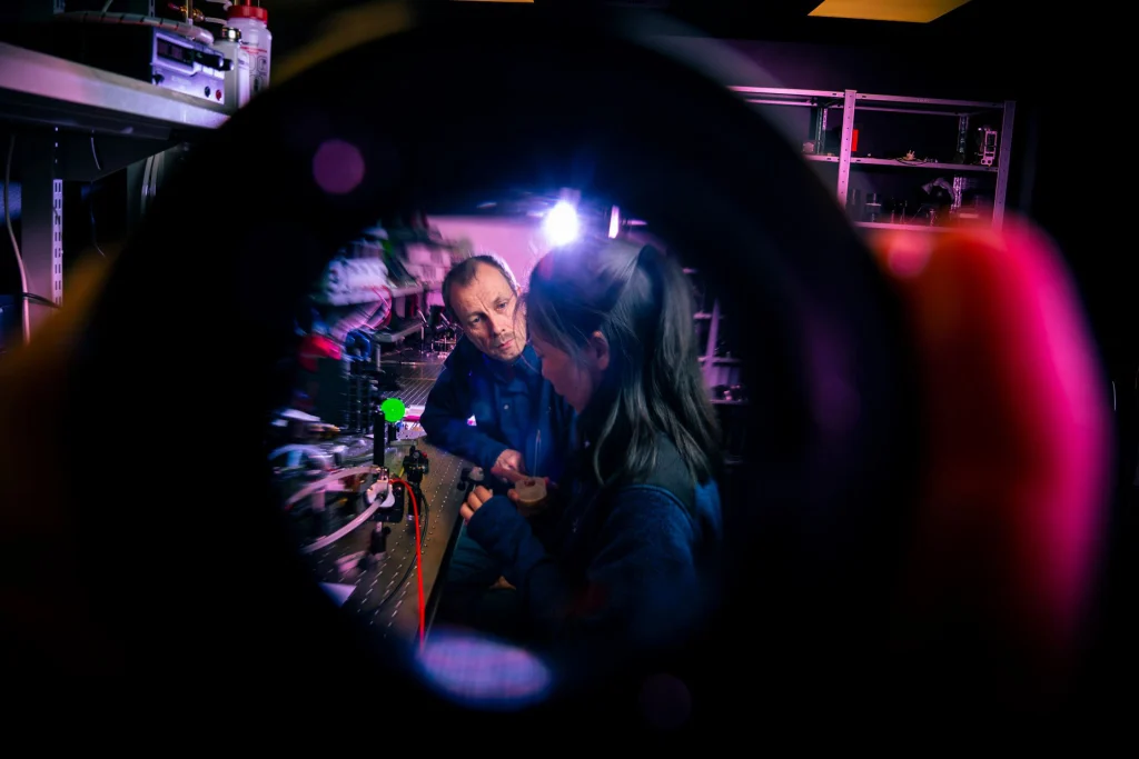
Masks are the past
Maskless DLP-based exposure means zero physical masks to procure, store or replace. Change the design at 2 PM, run production at 3 PM.
Vertically integrated
Every critical element under one roof — tighter tolerances, faster iteration and complete system optimisation that bolt-together solutions cannot match.
Field-proven partner
The industry standard for high-throughput Direct Imaging — running 24/7 in PCB, advanced packaging and semicon production worldwide.

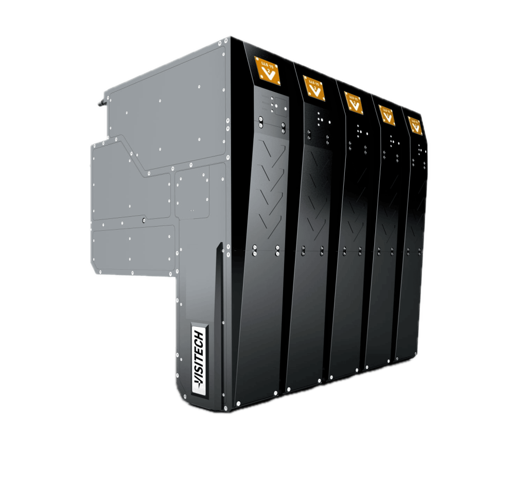
Engineered in-house.
Deployed and supported worldwide.
- Years of DLP experience
- 25+
- Systems deployed
- 15 000+
- Field-proven reliability
- 24/7
LED or laser — which should I choose
It follows your resist and your target line. The 4-peak LED switches between 365, 380, 395 and 405 nm and suits broader-band resists; the laser reaches the finest features and i-line chemistry. The LLS06 is the head in this range where both are offered.
Where does 720 wafers an hour place the LLS06?
It is the highest throughput in the fine half of the lineup, at 6 µm line/space. On 515 × 510 mm panels the figure is 240 an hour. Figures are for discussion and confirmed per resist and energy density.
Is the alignment camera included
It is an option on the LLS06, where the finer heads carry it as standard. Whether you need it is a question about your registration budget, not about the head.
Which panel formats does it take
310 × 310, 510 × 515 and 600 × 600 mm, with no theoretical maximum panel size across the LLS range.
Can a process move between the LLS06 and a finer head
Yes — every LLS photohead runs the same LURIA platform, so a recipe proven on one carries to the next.
Not sure which head?
Tell us your line, panel and volume
Send the resist, the target line / space and the format, and a field application engineer comes back with a recommended photohead and a configuration to design around — usually within two business days.
- NorwayHQ · Drammen
- ChinaShanghai
- United StatesAllen, TX
- JapanTokyo