
LUXBEAM® LLS15
HDI and fineline PCB at 15 µm
A 405 nm laser or 4-peak LED photohead for HDI, mSAP, inner layer and flex — on 510 × 515 and 600 × 600 mm panels and the large formats PCB production actually runs.
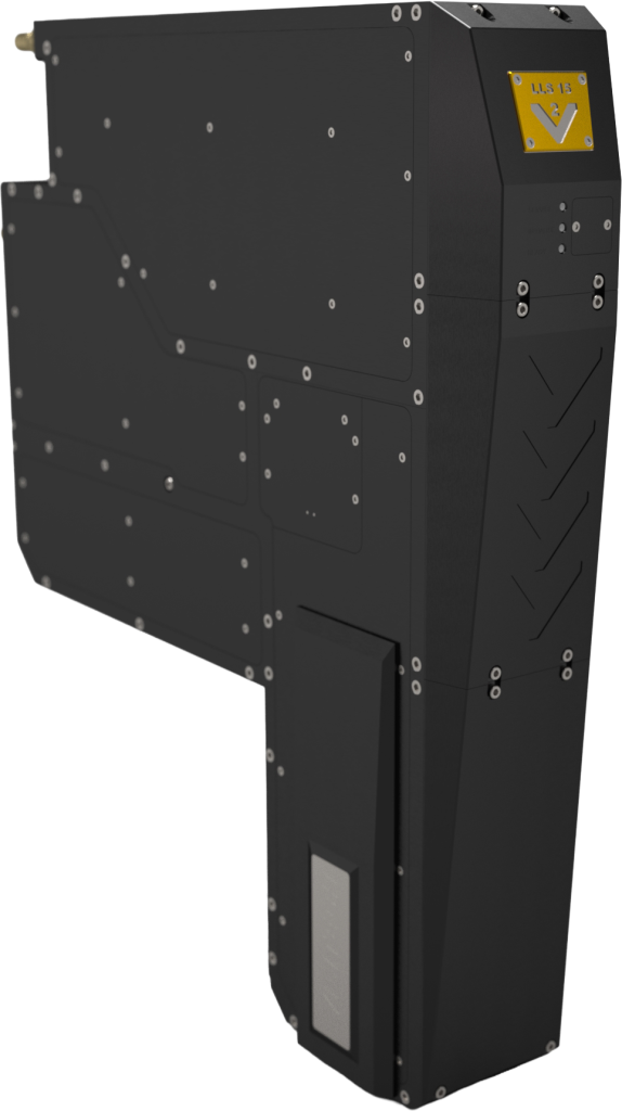
What sets it apart
LLS15 — in three numbers
-
15 µm line and space
Above 90% CD uniformity, with the alignment camera as an option.
-
405 nm laser or 4-peak LED
Pick the source your resist wants: a single laser line, or 365 / 380 / 395 / 405 nm switchable LED.
-
About 8 s a side
On a 515 × 510 mm panel — PCB-line cadence at fineline resolution.
Application fit
Where LLS15 fits
HDI and mSAP
High-density interconnect and modified semi-additive process, at panel scale.
Inner layer and fineline
Inner-layer imaging, and selective fineline where only part of the panel needs it.
RF and antenna-in-package
Geometry where edge definition is the specification.
Flex
Flexible circuits, where the substrate moves and the pattern has to follow it.
Specifications
LLS15 — at a glance
Imaging & Layout
- Resolution
- 15 µm
- Light source
- 405 nm laser, or 4-peak LED
- Throughput — 515 × 510 mm panel
- ~8 s/side
- Typical applications
- HDI, mSAP, inner layer, fine-line (selective), RF / antenna-in-package, flex
- Substrate / panel
- 510×515, 600×600, large PCB
- Segment
- PCB
Integration
- Cooling
- Liquid
- Pattern formats
- GDSII · OASIS · ODB++ · Gerber
- Real-time features
- Positioning · scaling · rotation · warping · re-routing · autofocus
Figures are for discussion and to be confirmed per application. Throughput depends on resist and energy density — send us both and a field application engineer will verify them for your process.
Why Visitech
We engineer the imaging heart
inside your next machine
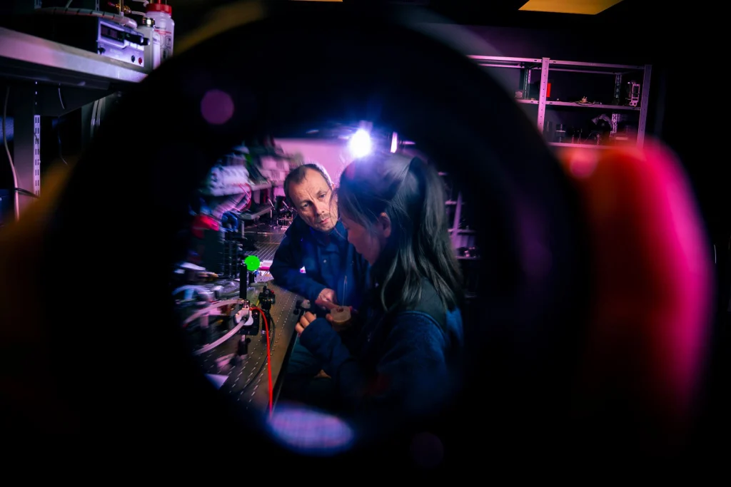
Masks are the past
Maskless DLP-based exposure means zero physical masks to procure, store or replace. Change the design at 2 PM, run production at 3 PM.
Vertically integrated
Every critical element under one roof — tighter tolerances, faster iteration and complete system optimisation that bolt-together solutions cannot match.
Field-proven partner
The industry standard for high-throughput Direct Imaging — running 24/7 in PCB, advanced packaging and semicon production worldwide.

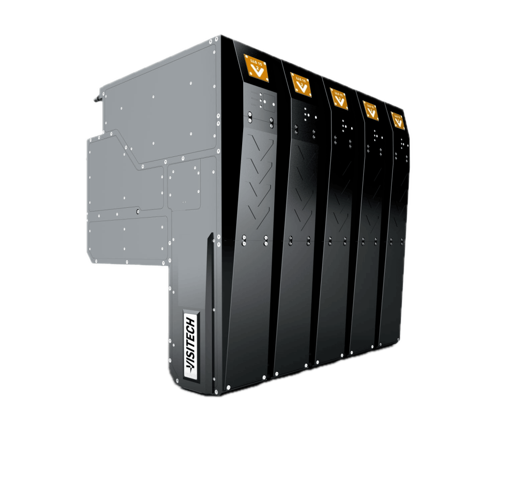
Engineered in-house.
Deployed and supported worldwide.
- Years of DLP experience
- 25+
- Systems deployed
- 15 000+
- Field-proven reliability
- 24/7
Where does the LLS15 sit in the lineup
At 15 µm line and space — the fineline end of PCB. Below it the LLS06 reaches 6 µm for advanced packaging; above it the LLS30 covers solder mask and standard PCB at 30 µm.
LED or laser
Both are offered: a 405 nm laser, or a 4-peak LED switching between 365, 380, 395 and 405 nm. The choice follows your resist.
What throughput should I plan for
About 8 seconds a side on a 515 × 510 mm panel. Real numbers depend on resist and energy density.
How large a panel can it image
510 × 515 and 600 × 600 mm, and the large PCB formats above them — there is no theoretical maximum panel size across the LLS range.
Does it handle flex and warped panels
Yes. LURIA reads the substrate before every exposure and adapts the artwork in real time — scaling, rotating, warping and re-routing — which is what makes flex and high-warp panels patternable at this line width.
Not sure which head?
Tell us your line, panel and volume
Send the resist, the target line / space and the format, and a field application engineer comes back with a recommended photohead and a configuration to design around — usually within two business days.
- NorwayHQ · Drammen
- ChinaShanghai
- United StatesAllen, TX
- JapanTokyo